

Part 2: Remote Battery Monitoring - PIC16-based Display Subsystem
Date : 16 Sept 2024GIT Repository : view
Posted on : 16 Sep 2024
Tag(s) : PIC16F1459, Shift-Registers, Remote-Monitoring, XC8
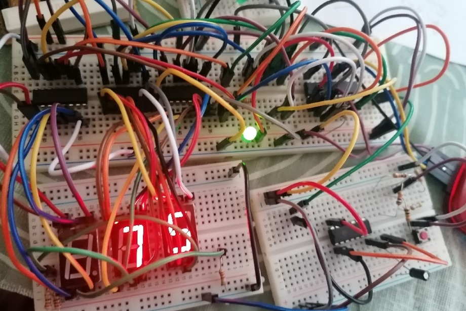
Welcome back to the remote battery monitoring project! In this article, we continue by building a new subsystem to display the battery level on three single-digit 7-segment displays. A key focus of this design is to minimize power consumption and reduce the overall cost of the subsystem. This article specifically covers the display subsystem, while other components will be explored in future installments as we expand on this project.
Design Overview
For this subsystem, we’ll use the PIC16F149 microcontroller due to its low cost and because it is available in a 20-pin package. This microcontroller supports SPI interfacing, which will be useful later when connecting the display subsystem to a master controller. To further optimize power usage, the subsystem will only display the battery level for a short period before entering sleep mode. An external interrupt triggered by a push button will wake the system when the battery level needs to be viewed.
Displaying Digits
A 7-segment display is composed of seven LEDs arranged to form a digit. Each display requires seven pins to control the individual segments. But since we are using three 7-segment displays, we would need a total of 21 pins, which exceeds the available I/O pins on the PIC16F149. To resolve this, we’ll use shift registers to reduce the number of pins required.
A shift register is a sequential logic device that shifts data from input to output on each clock cycle. For our project, we’ll use an 8-bit serial-in, parallel-out shift register. This allows us to control a 7-segment display using only three pins per digit. It’s a neat solution for when the number of available pins is limited.
The timing diagram of a typical shift register is shown below:
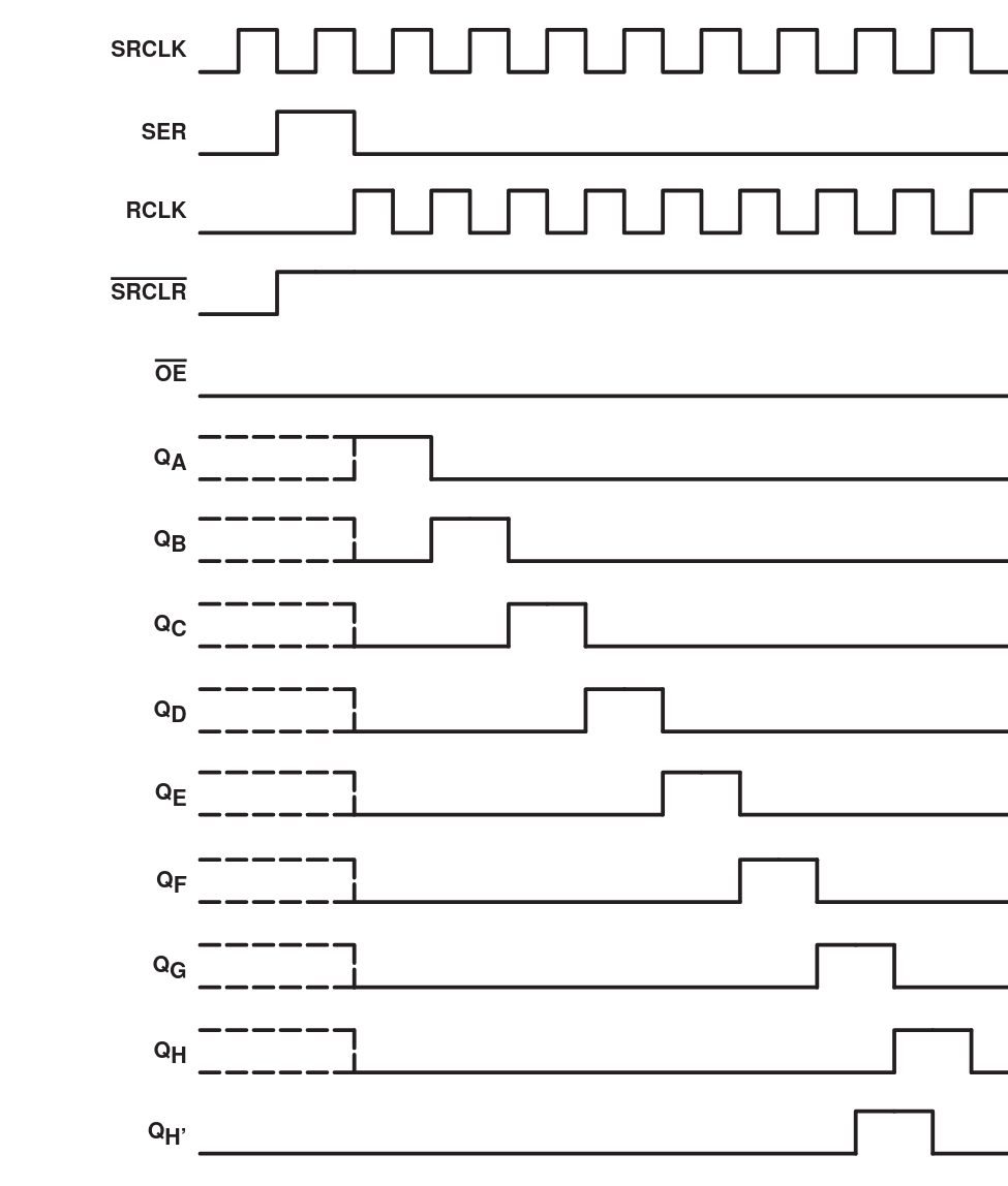
In this diagram, SRCLK represents the shift register clock signal, SER represents the input data bits, QA to QH represent the output bits, and RCLK is the clock signal to the latch. When the latch signal transitions from Low to High, the input bits of the shift register are transferred to the output pins.
By using this design, we can control all three 7-segment displays with just five pins on the microcontroller: two for clock and latch signals, and three for sending the data bits. This approach greatly simplifies the design while ensuring efficient use of the microcontroller pins.
Button Debouncing
To conserve power, we’ll only activate the display when needed. Upon pressing a push button, the microcontroller will wake up from sleep, display the battery level for about 10 seconds, and then return to sleep mode. The button press will generate an external interrupt to trigger this action.
However, we need to address the issue of button debouncing. When a button is pressed, it can generate multiple signals due to mechanical bouncing. To avoid triggering multiple interrupts, we’ll debounce the button using an external circuit—an RC filter with a Schmitt Trigger, which is more fun than a software solution!
Below is the circuit for debouncing the push button, using an RC filter and a Schmitt Trigger Hex inverter:
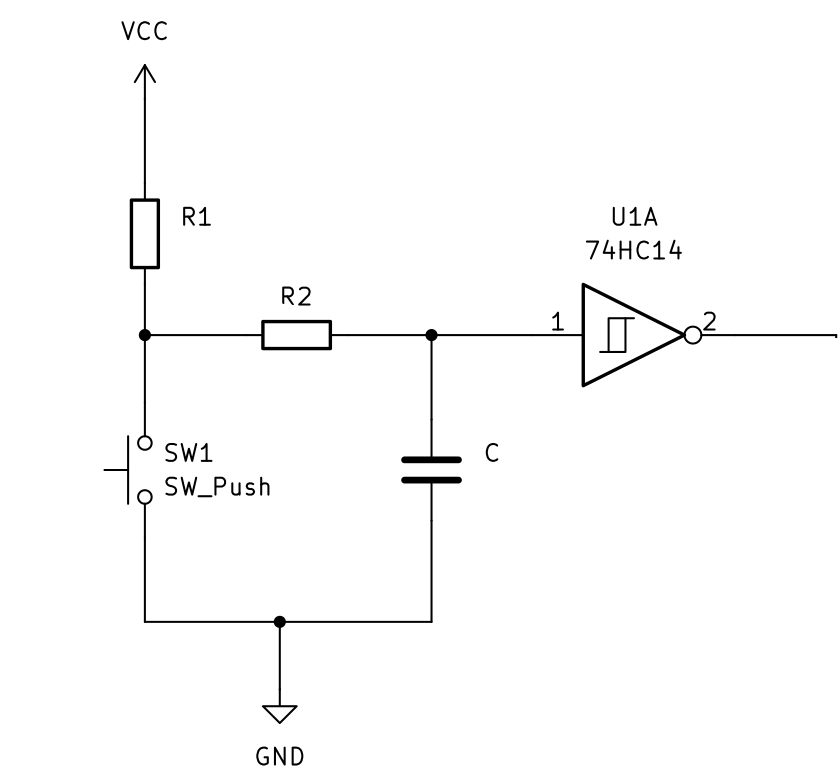
The Schmitt Trigger operates using hysteresis, reacting only when voltage changes exceed a certain threshold. This helps to ensure reliable signal transitions.
Debouncing Circuit Calculations
We use the following equation to calculate the capacitor’s discharge voltage:
$$ {V_{cap} = V_{init} (e ^ {-t \over RC } )} $$
Where Vcap is the capacitor voltage at time t, Vinit is the initial voltage, and RC is the time constant. In our circuit, R is the value of R2, and the Schmitt Trigger will change output when Vcap drops below the threshold voltage Vth. Therefore, to find R2, we can rearrange the equation as follows :
$$ {{ R = \frac{-t}{C [ ln(\frac{V_{th}}{V_{ini}}) ] } }} $$
For our design we can assume a bounce time of 20ms, with a Vth of 2.825 at 5.25V for the SN74HC14 based on a signal going low. Therefore R2 is :
$$ {{ R_2 = \frac{-20 \times 10^{-3}}{(1u) [ ln(\frac{2.45}{5}) ] } \\ R_2 = 35\: K\Omega }} $$
Similarly, we calculate R1 using the charging equation for the capacitor :
$$ {{ V_{th} = V_f \times (1 - e^ { \frac{-t}{(R1 + R2) \times C }}) }} $$
Provided Vth = 1.825V at 5.35V for the SN74HC14 Hex inverter for a signal going low to high, This results in
$$ {{R_1 = 9\: k\Omega}} $$
Circuit Diagram
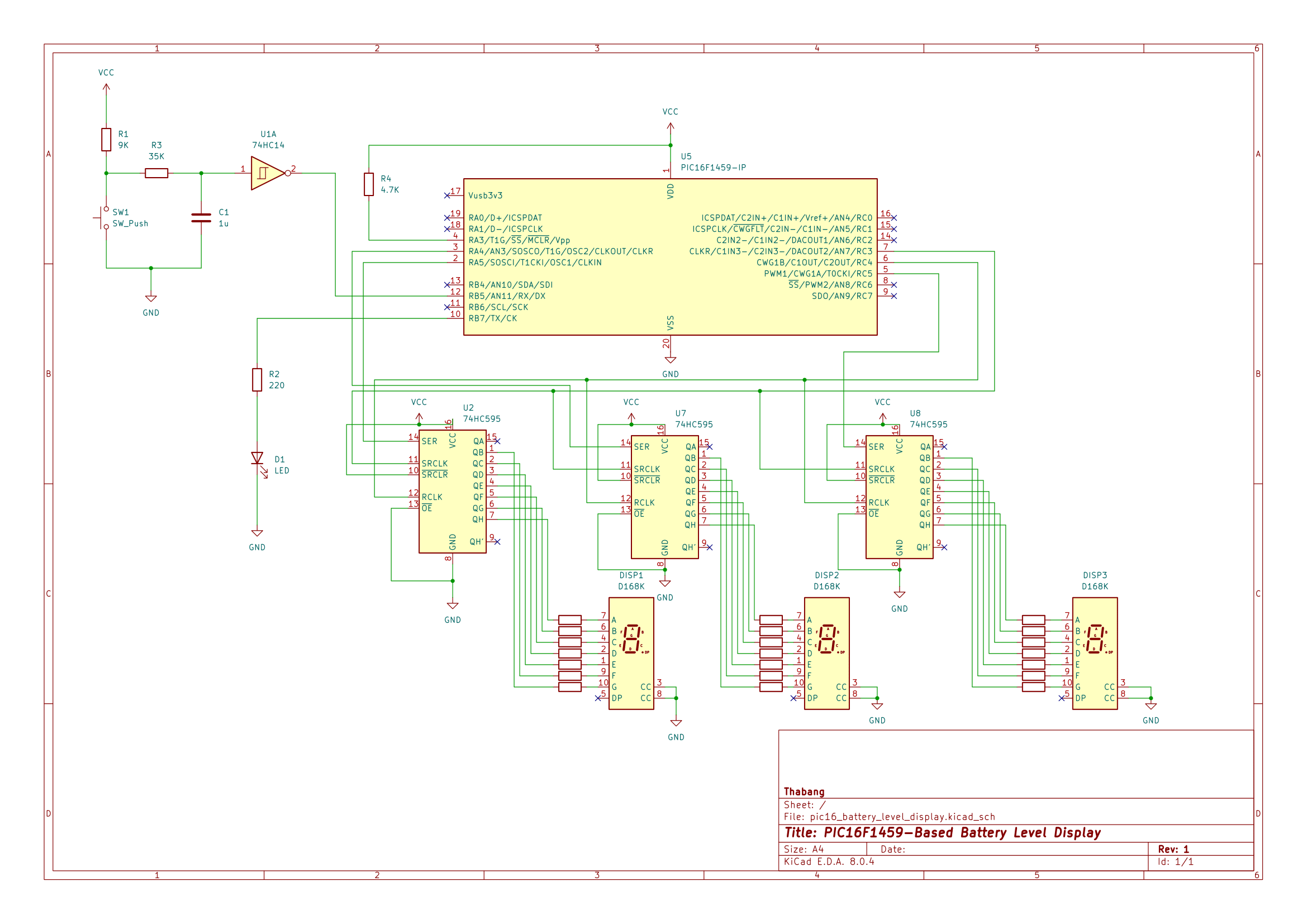
The schematic diagram of the complete display subsystem is shown below:
The Code
The source code for this project is available on my GitHub repository [here]. We are using MPLAB X IDE along with the XC8 compiler. In the main() function, we configure the PIC16F149 to use its internal 4 MHz oscillator. We set up pins RA5, RA4, RC5, etc., as digital outputs, with RB5 configured as a digital input for the button interrupt. The interrupt-on-change (IOC) feature is used to capture button presses, and upon triggering the interrupt, the display is activated to show the battery level.
Conclusion
In this article, we successfully designed and built the display subsystem for our remote battery monitoring project. By leveraging shift registers, we minimized the number of microcontroller pins needed to control multiple 7-segment displays. Additionally, we implemented a hardware debouncing solution to ensure reliable button presses. In future articles, we’ll integrate this subsystem with the master controller and explore communication between the subsystems. Stay tuned!
Other links related to this project
- ESP8266-Based Remote Battery Monitoring and Low-Level Indication : Part 1