


Real-time Voltage Sampler using PIC18 and Persistent EEPROM Storage
GIT Repository : viewPosted on : 30 Dec 2024
Tag(s) : PIC18, EEPROM, I2C
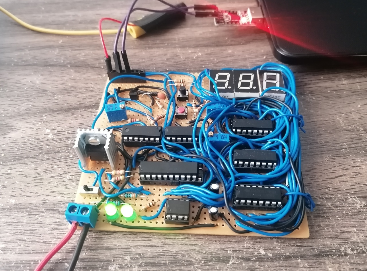
This project focuses on building a real-time periodic voltage sampler with multiple modes of operation. The device is ideal for monitoring DC voltages over time, such as battery voltages. It is built to save voltage samples into permanent EEPROM memory for later retrieval and can also transfer voltage samples to a serial device, such as a PC, for real-time monitoring.
System Overview
The hardware diagram for the system is shown below:
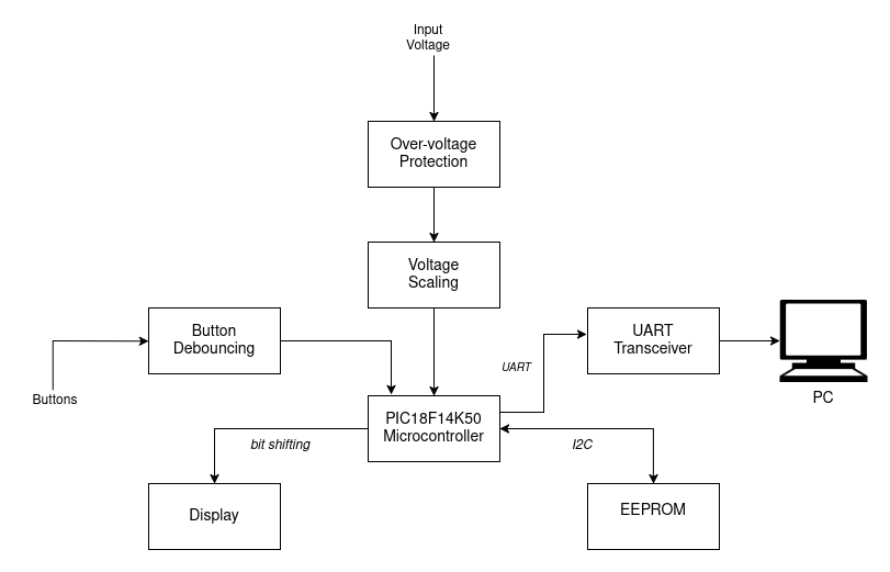
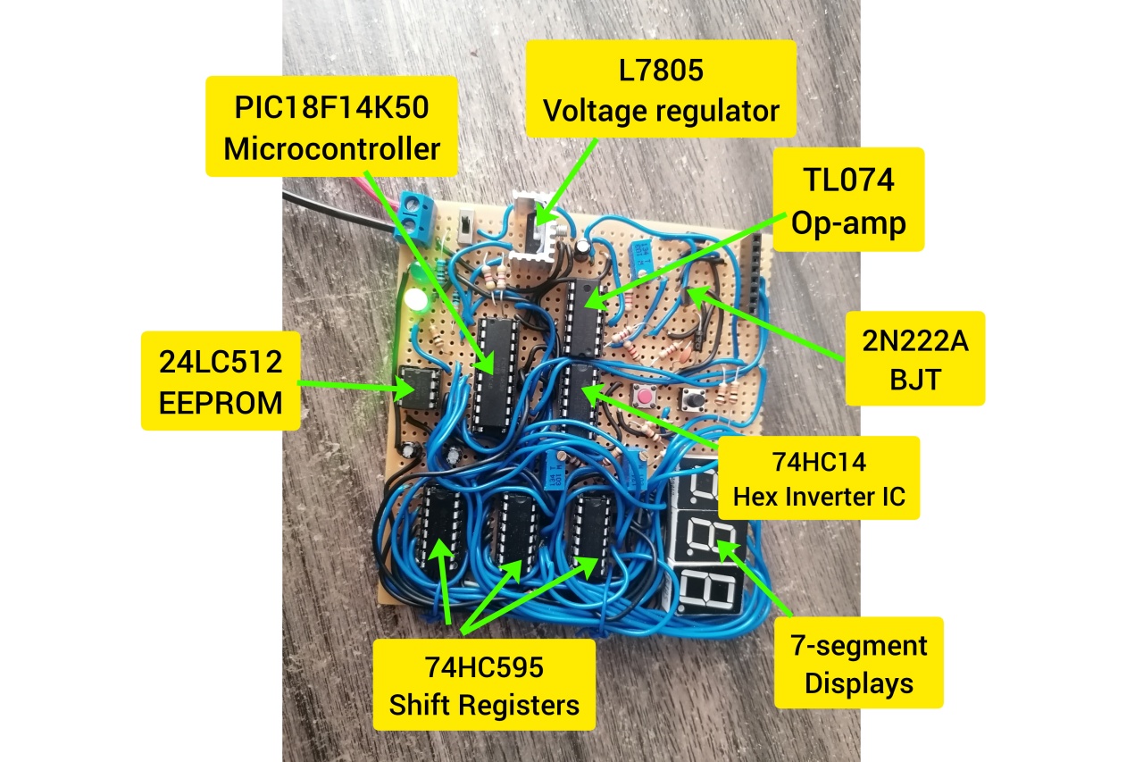
The system consists of several subsystems that interact to perform the desired functionality. The input voltage is processed through an overvoltage protection subsystem to ensure it stays within the 0–10V range. This voltage is then scaled down and fed to the ADC of the PIC18F14K50 microcontroller for sampling.
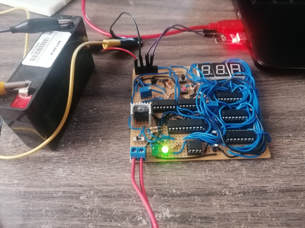
The microcontroller uses two push buttons for mode selection, and the buttons are debounced in both hardware and software. Three 7-segment displays provide a user interface, while UART communication is used to transmit data to a PC. Furthermore, Voltage samples are stored in an external EEPROM via the I2C protocol.
Hardware Details
Overvoltage Protection and ADC Voltage Scaling
The input voltage is limited to the ADC's safe operating range through the circuit shown below :
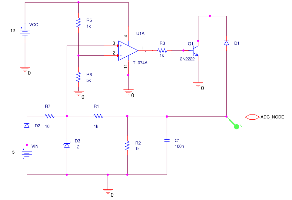
- Voltage Divider: Resistors R1 and R2 scale down the input voltage to a suitable level for the ADC.
- Low-Pass Filter: Capacitor C1 forms a passive low-pass filter with the voltage divider to improve the ADC's accuracy by filtering high-frequency noise.
- Resistors R5 and R6 set a reference voltage of 10V at the inverting input of the op-amp.
- When the input voltage exceeds this 10V threshold, the op-amp output transitions from low to high, activating the transistor Q1.
- Current flows from the transistor's collector to the emitter (ground), effectively clamping the voltage across C1 to a safe level for the ADC.
This design ensures that the ADC is protected from overvoltage conditions while maintaining high accuracy for voltage sampling. It ensures that the voltage across the ADC pin of the microcontroller never exceeds 5V. Furthermore, The Zener diode D3 serves to clamp down voltages exceeding VCC (12V). A DC simulation of the voltage across C1 as the input voltage (VIN) is sweeped from 0V to 20V is given below:
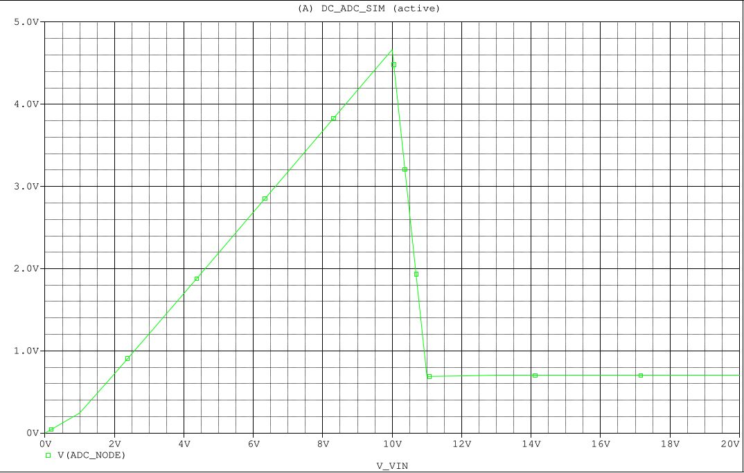
As can be seen from the figure above, the input voltage is first clamped by the op-amp circuit when it exceeds 10V but is below the VCC rail voltage. When it exceeds VCC, the zener diode D3 will conduct to keep the voltage below 12V.
Button Debouncing and Display
Push buttons are debounced using an RC filter circuit and a Schmitt trigger hex inverter, ensuring stable operation. The display subsystem features three 7-segment displays controlled via serial shift registers, providing clear output for various operational modes.
More details on debouncing and display designEEPROM Storage via I2C Protocol
The EEPROM (24LC512) is interfaced via the PIC18's MSSP module using I2C communication. To configure and use I2C on the PIC18, there are 4 main registers of interest. These are SSPADD, SSPCON1, SSPCON2, and SSPSTAT. SSPADD is used to set the baud-rate for our I2C communication. The formula used is shown below:
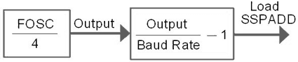
For this project, FOSC = 2 MHz, and we shall use 100 KHz as our I2C clock frequency for communication with the EEPROM. Thus, the SSPADD value is 2.
SSPCON1 and SSPCON2 are the control registers, whereas SSPSTAT is the status register that is monitored to check for various flags during transmission and reception of data from the I2C bus.
The 24LC512 EEPROM is a 512 Kbit device. This means we have a storage capacity of 64, 000 bytes. The I2C addressing for this slave device is shown below:
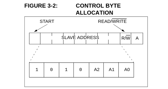
The pins A0, A1, and A2 on the device set the slave address. For this project all pins are grounded, so the device will have an address of 000. The full 7bit slave address is thus 1010-000.
Software Details
ADC Sampling
The ADC operates in two modes:- Passive Mode: Samples are stored in EEPROM for later analysis, taken every minute to optimize storage.
- Active Mode: Samples are transmitted via UART for real-time monitoring.
The ADC sampling is accomplished through a timer-routine. Timer 1 on the device is configured for a clock period of 1.04 seconds. The formula for calculating the Timer period is shown below:
$$ \text{Timer 1 period} = 1 \div \frac{F_{osc}}{4 * Prescaler * 2^{n}} $$
For Fosc = 2MHz and prescaler of 8 we get a period of 1.048 seconds.
For our passive-mode sampling, the ADC takes voltage samples every 59.76 seconds (roughly 1 minute). This means, in 24 hours we will have roughly 1440 samples. This limit can be increased, however the purpose of the slow sampling rate is to optimize available storage so it does not run out quickly.
With the current configuration, redundant bytes are added after every 16-bit value to ensure data integrity. This is illustrated below :
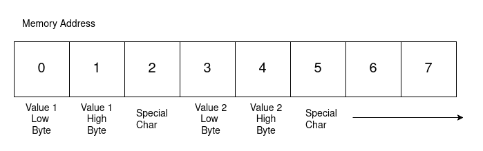
The ADC values are stored as 16-bit values on the EEPROM, this means our data storage throughput is 1/3 = 33 %. Our passive-mode sampling will produce roughly 1440 samples per day, Therefore, the 512 Kbit EEPROM will run out of storage in $$ 512\:kbit * \frac{1\:byte}{8 bit} \times \frac{1}{3} \times \frac{1\:day}{1440\:byte} = \text{14 days}. $$
If using a 64 Kbit EEPROM, then we run out of storage in 1.85 days. The voltage sampling rate and the EEPROM size can be adjusted as required to serve different needs.
Finite State Machine
The finite state machine (FSM) for the system is shown below.
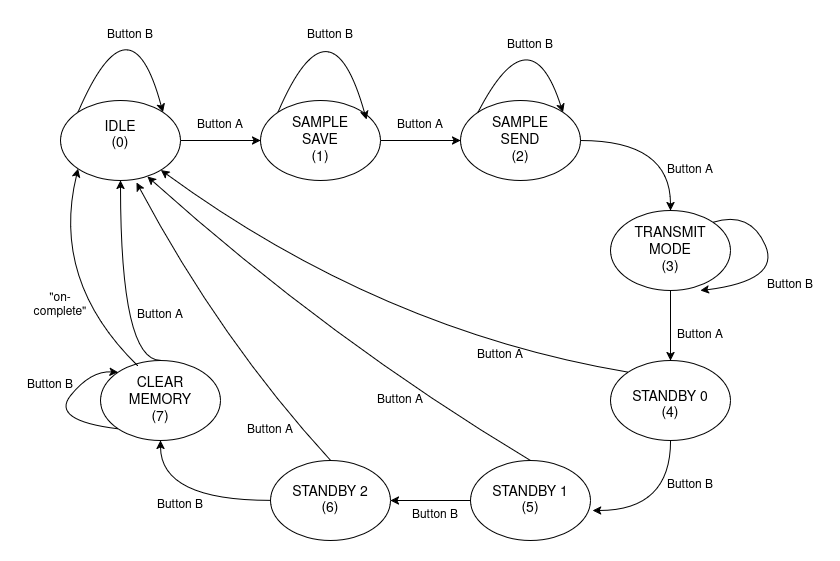
The push buttons ( Button A and Button B) are used to navigate between the different states of the device. These states are described below:
-
State 0: Idle
In this state, the device is idle and performs no active functions. If the display is turned on, it will show the character "A".
-
State 1: Passive-Mode Sampling (sample save)
The device periodically takes ADC samples and saves them to EEPROM storage. When the display is turned on, it will show the most recent voltage sample in fixed-point notation, such as 0.72 or 3.25.
-
State 2: Active-Mode Sampling (sample send)
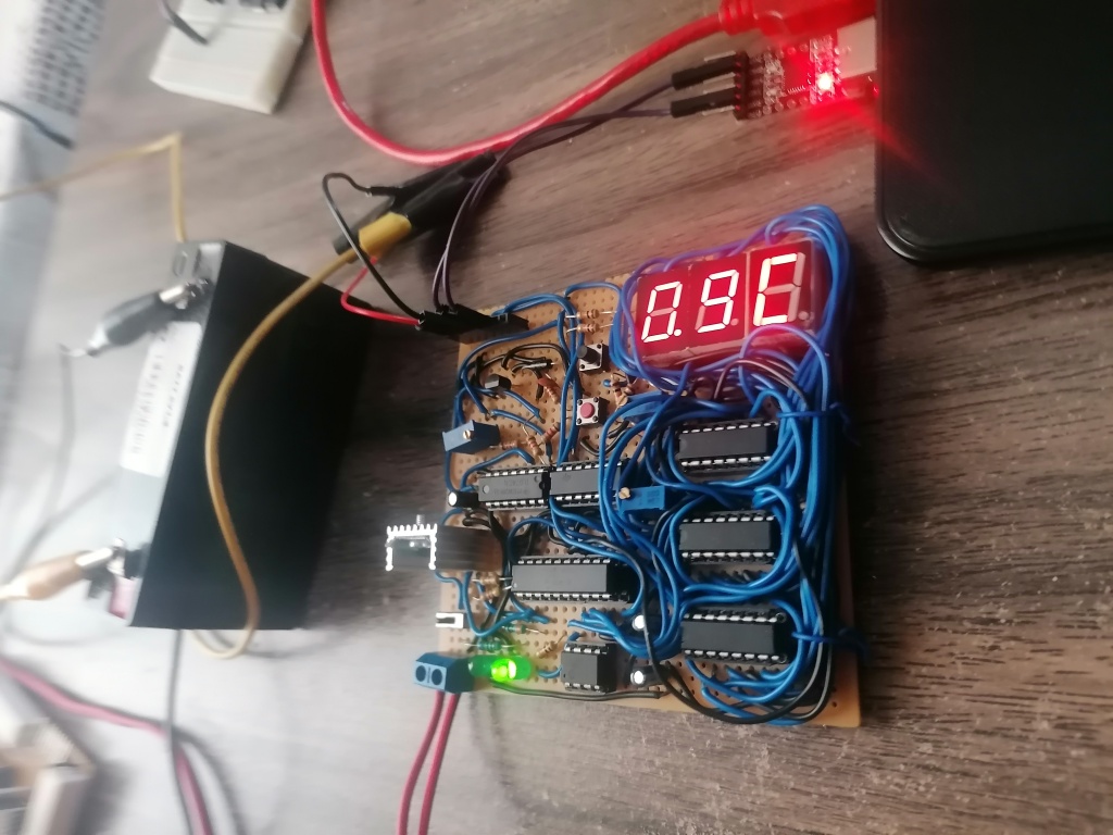
In this state, the device takes ADC samples and transmits them via the UART interface for real-time monitoring. If the display is turned on, it will show the most recent voltage sample followed by the character "C", e.g., 0.7C or 3.2C.
-
State 3: Transmit Mode
The device reads data from the EEPROM starting at address 0 and transmits it via the UART interface. When the last address is reached, the device loops back to the beginning and continuously transmits all stored data. The display shows the character "C" in this mode.
-
State 4: Standby Mode 0
This is a standby state for entering the clear-memory sequence. If ButtonA is pressed, the device exits this state. If ButtonB is pressed, the device moves to the next standby state in the sequence.
-
State 5: Standby Mode 1
Another standby state for the clear-memory sequence. The device remains idle, awaiting confirmation to move to the next state.
-
State 6: Standby Mode 2
The final standby state before entering the clear-memory state. The device remains idle, awaiting confirmation to proceed.
-
State 7: Clear Memory
In this state, the device clears all data stored in the EEPROM and fills all registers with null values ( 0). The display shows the characters "CLR", and a connected LED flashes continuously until the operation is complete and the device exits this state.
Software Code
The complete software code is available on my GitHub repository. The project code is for MPLAB X IDE with XC8 compiler.
Conclusion
This project demonstrates the design and building of a real-time periodic voltage sampler with multiple modes of operation. The device is ideal for monitoring DC voltages over time, such as battery voltages.
Video Demonstration
Watch the switching of the operation modes in action :
References
- Part 2: Remote Battery Monitoring - PIC16-based Display Subsystem : Part 2
- [1] : ElectronicWings, "PIC18F4550 I2C - Introduction to I2C protocol" , https://www.electronicwings.com/pic/pic18f4550-i2c
- [2] : Microchip, "24LC512 EEPROM Datasheet", https://www.microchip.com/en-us/product/24LC512